1. Conductors
Posses free elect
rons
Metals are all good conductors due to having low resistance to the flow of current.
2. Insulators
They do not have free electrons for conduction. They have high resistance to the flow of current.
All non metals are bad conductors. Eg. dry wood, paper and air.
3. Semiconductors
These are class of materials whose conductivity is between that of good conductors and insulators
Silicon and Germanium are examples of semiconductors elements widely used in electronic industry.
INTRINSIC SEMICONDUCTORS
These are pure semiconductors.
EXTRINSIC SEMICONDUCTORS
These are impure semi conductors material.
DOPING
Is a process of introducing a tiny amount of impurity into a semiconductors material to form extrinsic semiconductors shells.
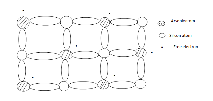
N-SEMI CONDUCTORS
–Silicon and germanium atoms are tetravalent
-They have four electrons in their outermost shell.
-When a doner atom with fine electrons in its outer most shell (ie Arsenic) is added to a silicon crystal, the fifth electrons becomes a free change carriers since there is production of large number of negative charge carriers(electrons) the impure semiconductors is called N-Semiconductors
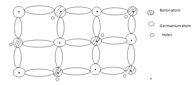
P-SEMICONDUCTORS
A-P- Semiconductor is made by adding a trivalent atom (an acceptor) such as B or on to pure semi conductor such as germanium. Since there is a production of large number of holes (positive charges) the impure semiconductor is called P- Semiconductor.
P-N=JUNCTION/DIODE:
This is formed when P and N semiconductors are melted to form a junction between them
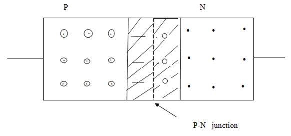
The marrow region at the P-n junction which contains the negative and positive charge is called depletion layer.
A barrier dip is a p.d which oppose more diffusion of charges across the junction.
This is produced when the flow of +ve and -ve Charges ceases
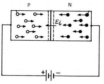
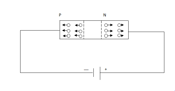
P – N JUNCTION AS A RECTIFIER:
FORWARD BIAS.
Is said to be forward biased when its P- semiconductor is connected to the +ve terminals of the battery and its N- Semi conductors is connected to the -ve terminal at the battery.
In this case electrons and holes flow across the P-n junction. This happen because the +ve pole of the battery repel the +ve charge and –Ve pole rel the –ve charges.
REVERSE BIAS
A-P-N junction is said to be reverse biased when its P. Semiconductor is connected to the negative pole junction of a battery and N. Semiconductor is connected to the +ve [p;e pf the battery in this case only a very small a current flows.
P-N JUNCTION AS RECTIFIERS
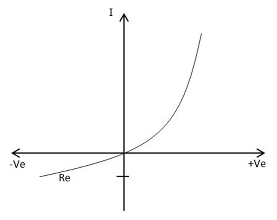
The graph shows that P-N junction acts as a rectifier, it has low resistance in one direction of P.d (ie + v) and higher resistance in the opposite direction of P.d (-v)