Common collector configuration
Under this configuration the transistor has current gain but no voltage gain
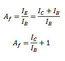
 =Amplification factor
 =
=
 =
=
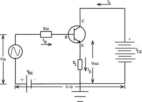

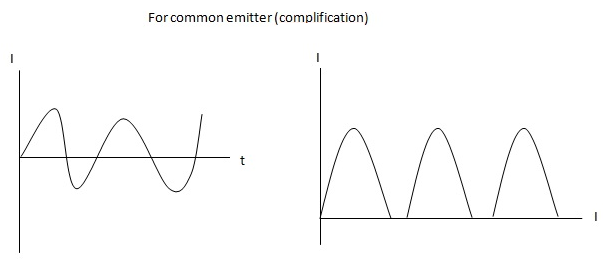
For common emitter
Vo = IC R2
Vi = IBRB
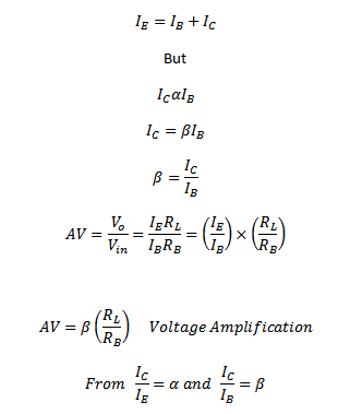
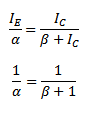
From, IE = IB + IC


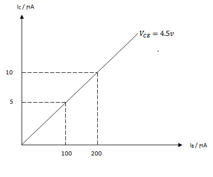
Common emitter characteristic curve
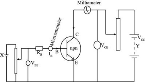
The circuit above is for investigating the variation of current with voltage in the input and output circuits.
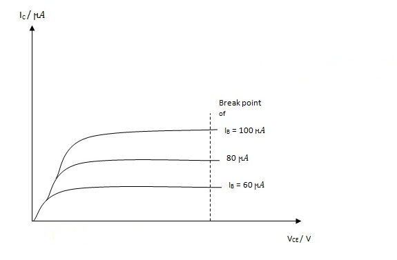
OUTPUT CHARACTERISTICS
IC-VCE with IB constant .
The results are plotted below.
The knee of the curves shown corresponds to a low P.d(0.2) the output for higher P.d the output IC varies linearly with VCE for a given value of base current IB.
The linear part of the characteristic is the one used in the audio frequency (a.f) amplifiercircuits so that the output is undistorted.
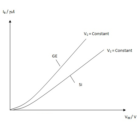
INPUT CHARACTERISTICS
IB-VBE with VCE constant
The results are as follows:-
The input characteristics is non-linear
TRANSFER CHARACTERISTICS
IC-IB with VCE constant
The results are as shown below:-
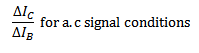
The output current IC varies linearly with the input current IB. The current transfer ratio or current gain is given by
In the figure below

Questions
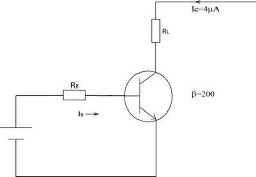
1. An npn transistor has a current gain (Beta) value of 200. Calculate the base current  required to switch a resister of 4µA.
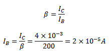

2. An npn transistor has a dc base bias voltage  of and an input base resistor
  of 100kΩ.What will be the of base current into the transistor
(The transistor is a silicon type)
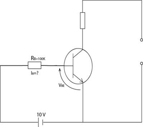
Data
From Kirchhoff law
law
For silicon
 =10v
=10v
 = 100kΩ
 =0.6v (wasted voltage)
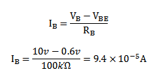
Solution
 –
– –
– =0
=0
 –
– =
=
Example
Given the circuit below, determine
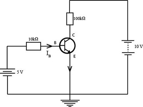


The transistor has  =150
=150
The transistor of silicon type
Solution
Second Kirchhoff’s law in the input circuit
 ×
× = 0
= 0
5V

 A
A
 A
A


 =0.6v
=0.6v

10
 = 3.4V

 =5+ (
=5+ (  )
)
 =5+ (10000×4.4×10-4)
  (6.6)
(6.6)
 =2.8v
=2.8v