Example
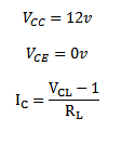
1. A common emitter amplifier has  = 1.2kÎ and supply Voltage of V=12v. Calculate the maximum collector current
  following throughout resistor when switched fully on (saturation assume
 .Also find
  with a voltage drop of 1v across it, the transistor silicon.
Solution


 A
A
Quiescent point:
It’s a point when the current flow is smooth i.e. not being clicked (excess) and transistor functions.
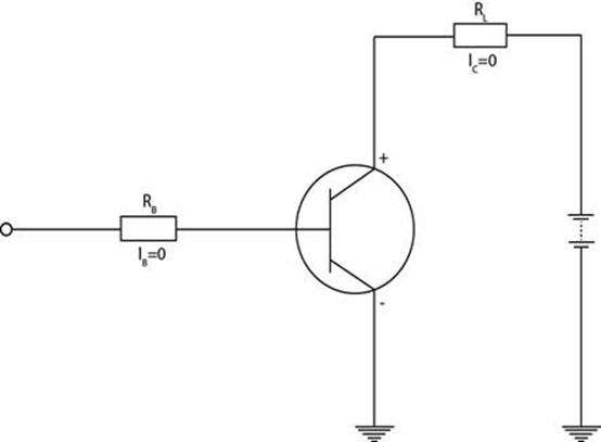
Saturation point:
If  =0 transistor is in the cutoff region, there is a small current collector leakage, CEO
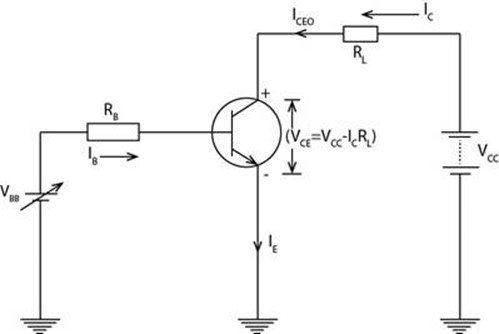
Normally  is neglected so that
 =
=
In cutoff both the base emitter and base collector junction are reverse based.
When base emitter becomes forward based.  is increase, then IC also increases when
  decreases as a result.
When  reaches its saturation value BC junction becomes forward based and
  can increase no further even with continued increase in
At the point of saturation ( ) not longer valid)
VCE(Sat) for a transistor occurs somewhere below the knees of the collector curve.
The saturation value for  (Sat) is usually a few tenth of volt for silicon transistors.
The DC load line, the cutoff and saturation can be illustrated by the load line.
Between the cutoff point and the saturation point is where the transistor is active and as most active at the quiescent point.
Self biasing /fixed bias
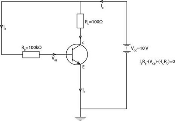


Outer loop


 A
A


 A
A

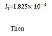
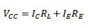
10 = 9.4×10-3×100 + 
 = 9.06V
Common emitter amplifier circuit
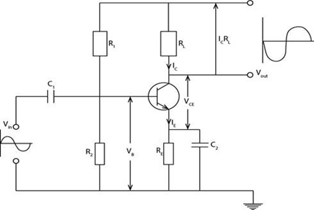
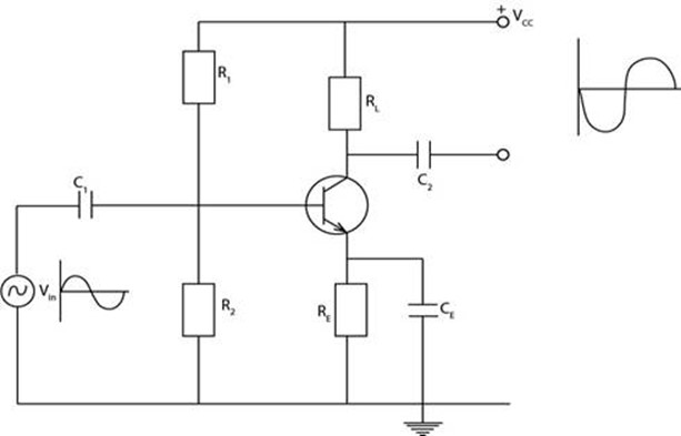


Faithful amplification- is the application or the output that is not distorted.
Question
a) Pd across base resistor
Consider loop (L), from Kirchhoff’s law
3V =0 but
  =0.7
=0.7
 = 2.3V
b) From Ohms law
 =
=
 =
=
 = 1.53
 =
= +
+ 
 =
=  ) + (
) + (
 = (20- 3) + (2.3-1.836)
 = (17+0.463)
 =17.463v
d) Find 
From Kirchhoff’s law
Given
 –
– –
– =0
=0
β=20
 =20v
=20v
So
20v-(1.5 ×1.224
 –
– =0
=0
 =18.164v
2.  Q
Q =
=  =
=

 =
= +
+
 = 25V
= 25V
 = 47mA = 4.7×10 -2A
 =
= 
=
 =0.3659Ω
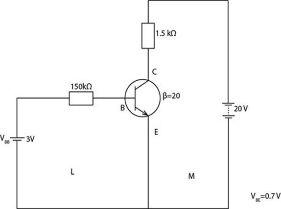
Question
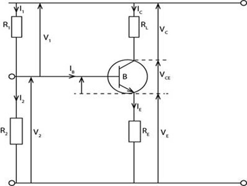
For the circuit above the transistor has a current gain  =80 the collector supply voltage
 = 40 .
The required biased conditions are  = 0.7V and
  = 1mA. Determine the suitable values for resistors
 ,
, ,
, &
&  ,
,
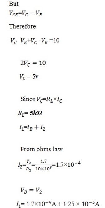
R2 = 10RE, VE = 1
VE = IV.
Given 
 v
v
 = 1×10 -3A
 =80
=80
 =0.0000125
 =
= = 0.0010A
 =1kΩ
=1kΩ
 =1
=1 10
10


 = 1.7 but

 +
+  =10
=10